
In Part 1 of this series, we explored some of the reasons you might want to use an FPGA instead of or along with an MCU. We also looked at a couple good introductory mainstream FPGA development boards.
In this episode, we’re going to start examining the process of creating FPGA designs. Contrary to what you may have heard, you don’t need to be an EE to do interesting things with an FPGA.
FGPAs require a Hardware Definition Language (HDL) that describes the structure and behavior of the digital logic circuits that will be created. The 2 most common HDLs are Verilog and VHDL.
Verilog
Verilog syntax is similar ot C. It is concise, with limited data types and keywords and is also case-sensitive and loosely typed. Verilog tends to be more popular in the US and China.
SystemVerilog is just a more updated version of Verilog. Most modern FPGA tools will support either flavor. If you have a choice between the two, choose a the more modern SystemVerilog version.
VHDL
VHDL stands for “Very High Speed Integrated Circuit Hardware Definition Language” – but no one ever calls it that. It has a syntax more similar to Ada or Pascal. It’s more verbose, with more datatypes and generally requires more typing for the same constructs when compared to Verilog. It is not case-sensitive and is strongly-typed. VHDL is more popular in Europe.
Most tools will support a mix-and-match approach, so if you can intermingle Verilog and VHDL modules without any problems. It’s also not super-difficult to convert modules between the two if you like to keep everything in the same language.
HDL Modules
Modules are the core building blocks of HDL, much like classes in C++/C#/Java. Modules consist of:
- Port declarations (direction, type, name)
- Defined parameters (think constants) and other wires/variables
- Instance declarations of child modules (think composition / “has-a” in Object-Oriented Programming)
- Combinatorial logic (change output values), which can either be continuous or in response to specific signal changes
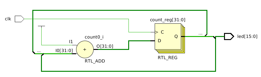
Here is a simple example of a Verilog module called “sample_top”. The “top” indicates that this is a top-level module, similar to “main” in C languages.
module blink_top(
    input clk,
    output [15:0] led
    );
   reg [31:0] count = 0;
   assign led[15:0] = count[31:15];

   always @ (posedge(clk)) count <= count + 1;
endmodule
In this module, there is 1 input and 16 ouputs. The first is the clock signal. A clock signal is just a heartbeat that goes high and low at a regular interval. It may or may not run at the same frequency as the main system clock. Depending on the FGPA speed grade, the main clock may run anywhere from tens of megahertz well into the gigahertz range. Clock dividers are commonly used to divide the main clock signal into lower frequencies used by different modules.
The second set of inputs is an array of 16 LEDs [15:0]. When the associated index/bit is 1, the LED is lit. As I mentioned in the previous article, the Basys3 has 16 built-in LEDs.
Compiling
FGPA projects are not actually compiled, but they still need to be converted to a format that can be run on the board.
- Synthesis: Turns HDL into a gate-level netlist of basic primitives (a list of what each low-level item is connected to.) Allows running of test benches/simulations and creation of a Register Transfer Level (RTL) schematic.
- Implementation: Translates from functional simulation netlist to timing netlist. Maps primitives to specific device resources. Place and Route process determines how device resources are located and interconnected inside the FPGA.
- Bitstream Generation: Specific to an individual FPGA model and creates a proprietary file format specific to the manufacturer.
Simulation
While you could go ahead and test our blink app by going through the full synthesize, implement, and bitstream generation cycle and then loading it to the board, it’s a better option to generate a test bench for it first. A test bench is simply a wrapper around your module that provides simulated inputs and records the outputs.
Why is this a good practice?
- Running a simulation is generally much faster than generating the file and loading it to the board as it avoids the lengthy implementation step. Simulations help you find and fix problems faster.
- The test bench becomes a unit/regression test for your module.
IfWhen you make changes to the module, the test bench will help to verify that the module still behaves as intended.
Luckily, HDLs provide great support for creating test benches. In fact, there are additional constructs in the language that are available only for simulation and are not synthesizable. The simulation only runs on your host computer – not the FPGA itself – so the test bench is free to use software commands that don’t translate directly to hardware.
Here’s a little test bench for our blink app:
module blink_top_tb();logic clk;logic [15:0] led;blink_top u_blink_top (.clk(clk),.led(led));always beginclk = 1'b1;#10;clk = 1'b0;#10;endendmodule
Notice that there are no inputs or outputs to the test bench. It creates logic elements (clk, led) for the module-under-test. In software speak, it creates an instance of the module-under-test and connects the test bench logic elements to the instance inputs and outputs.
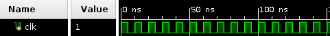
In the “always” block, it’s just creating a simulated clock signal, setting it to 1 (high) and waiting 10 simulated nanoseconds. Then it sets the clock to 0 (low) and waits another 10 simulated nanoseconds. It does this for as long as the simulation is set to run.
Here’s what the output looks like:
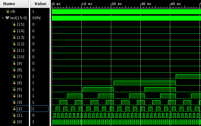
From the simulation output, you can see the LED outputs are just counting up, looking a lot like a clock divider with the period of each LED twice as long as the previous one. We’ve zoomed out (quite) a bit, so the clock shows as a solid bar since it has a 10ns period as shown earlier.
When programmed to the board, it looks like this:
On the Basys3, LED[0] is on the far right, and LED[15] is on the far left. The LEDs on the right are blinking, but so fast that they look solid. LED[6] is the first one that appears to be blinking to the naked eye. According to our sim output, this has a 20ms period.
This won’t win any innovation awards, but it shows how you can generate some interesting visual displays with only a few lines of HDL code and create a functional test bench.