
No man does it all by himself.
I said, young man, put your pride on the shelf.
– YMCA
My apologies the Village People, but now that the song is stuck in your head, let’s get on to the topic at hand: why you might want to invest time and money in learning to work with Field Programmable Gate Arrays.
I find that in talking to other software developers, a lot of them are pretty unfamiliar with what an FPGA is, so let me begin with an overly-simplistic definition. An FPGA allows you to create electronic circuits using a descriptive Hardware Definition Language (HDL). The HDL specifies how the inputs and outputs are connected, what the logic gates are, timing constraints, etc. in order to create an integrated circuit.
The hardest part for most software people to understand is that Central Processing Unit (CPU) and Microcontroller Unit (MCU) concepts such as “current instruction”, “stack”, and “heap” do not apply. Even though there are some HDL keywords that resemble standard C-style control structures, the end result is a series of circuits – not a set of instructions to be executed. From the outside, MCUs and FPGAs look a lot alike – but on the inside they are very different.
So why subject yourself to the paradigm shift that’s required to create an FPGA design?
- FPGAs let you solve certain problems that are difficult or impossible with traditional CPUs and MCUs. Chief among these are any tasks that require highly-parallelized execution.
- FPGAs let you create your own version of a microcontroller. For example, ARM provides Intellectual Property (IP) blocks that let you create your own Cortex M-series processor inside various FPGAs.
- FPGAs and MCUs complement each other nicely. This is the idea behind the System on Chip (SoC) boards that have become very popular. The MCU(s) handle the tasks that require complex state-dependent logic while the FPGA screams through the timing-dependent and/or highly-parallelized processing pipelines.
- FPGAs are a great way to increase your knowledge of of circuit behavior, logic gates, state machines, and low-level hardware protocols. Once you’ve implemented I2C in an FPGA, you’ll have a whole new level of understanding compared to simply using the Wire library in the Arduino IDE. That’s one reason they are commonly used in electrical engineering courses.
The good news is that that it has never been easier (or cheaper) to get into FPGA development than it is right now. Capable FPGAs are available for about the same price as a Raspberry Pi 4. Open source tools are available to avoid locking yourself in to a particular vendor or shelling out extra money for a design system.
But where to start? Let’s take a look at a few solid options for your first FPGA.
Digilent Basys3
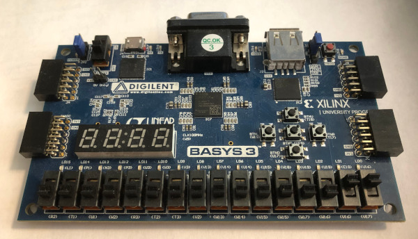
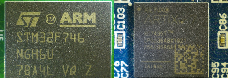
The Basys3 from Digilent is targeted at students and first-time FPGA users. It’s driven by the Xilinx Artix-7 XC7A35T FPGA. Let’s break down exactly what the heck that means.
- Xilinx: one of the industry and market-share leaders in FPGAs. They basically invented them.
- Artix-7: Artix is the low-power cost-sensitive FPGA line from Xilinx. A step up from the lowest-cost/lower-capability Spartan-7 family. The seventh series/generation of FPGAs.
- XC7A: Xilinx Commercial 7-series Artix
- 35T: # of logic cells / 1000 (actually, there are 33,280 logic cells, but I guess they rounded up) The smallest Artix-7 has 12.8k logic cells and the largest has over 200k.
- It also has 225K of RAM.
The reason you buy a trainer board though, is for the peripherals. It’s really handy to be able to use the on-board buttons, switches, LEDs, and connectors rather than having to wire up your own each time. It’s one less opportunity for things to go wrong and makes switching between different projects much easier. This is helpful if you tend to hop around between a number of different projects.
- Switches: 16 of them. You can treat them as individual on/off switches, or as a physical representation of a 16-bit register to control a single parameter with great precision.
- 16 LEDs: All green. One for each switch.
- 5 Buttons. The poor-man’s game pad.
- 4 Digit 7-Segment Display. Clocks, settings display, etc.
- VGA Port. Yes, VGA is pretty “old school”, but there are a lot of monitors that still support it. Plus, it’s way simpler and less demanding than HDMI – so it’s a good starter option for getting video out.
- 4 PMod Ports. PMod ports can be used with PMod peripherals or as general IO pins (48 of them) with your own jumper wires. There’s wide variety of PMod peripherals available from Digilent, but they are a bit pricy compared to other standard breakout boards with the same capabilities.
- USB HID Host: Handy for doing projects with a mouse or keyboard.
Basys3 also comes with a certificate that lets you register Vivado on your development machine. Vivado is the Xilinx integrated design suite for working with their FPGAs and SoCs. Stay tuned for a more in-depth look at this in a future post.
Basys3 product page on Digilent website
Terasic DE0-Nano
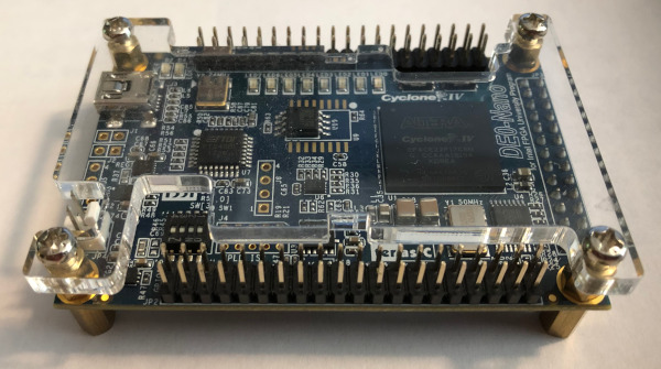
The DE0-Nano is more of a project board than a trainer board, due to it’s lack of peripherals. It’s powered by an Altera (Intel) Cyclone IV FPGA with 22K look up elements. It has 32MB of SDRAM and 106 IO pins. Intel / Altera is the second biggest vendor in the FPGA space, so this is still considered a “mainstream” board.
Peripherals include:
- 2 Buttons
- 4 Switches
- 8 LEDs (green)
- Accelerometer
The kit also includes a set of brass stand-offs/spacers, an acrylic shield, and a retractable micro-USB cable. The shield looks nice, but tends to be a bit of a nuisance in normal operation as it makes it difficult to get at the already-tiny buttons and dip switches.
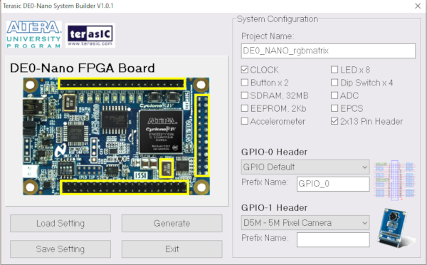
Intel provides the Lite edition of their Quartus Prime as a free download. It performs the same basic functions as Vivado does for the Artix-7, but how it does them is somewhat different. I hope to do a full comparison in the future, but some activities that were a bit troublesome in Vivado were much easier in Quartus Prime – especially regarding pin configurations and constraints. I like the System Builder tool that that Terasic provides with the board as it makes it easy to generate basic assignments .
DE0-Nano product page on Terasic website
Bottom Line
The Basys3 was my first FPGA and it’s worked really well for me. The 224K of RAM has been a bit limiting for certain audio and graphic limitations. The peripherals make it a great “jack of all trades, master of none” first choice to try out many different types of projects with minimal setup. This is generally my board of choice for trying out new ideas and techniques.
The DE0-Nano is about half the size and price of the Basys3. If you don’t mind hooking up your own peripherals for every project or you have a specific type of project in mind that would benefit from all it’s IO and memory, the DE0 is the more cost-effective option.
Comment (1) on "A Software Developer’s Guide to Getting Started with FPGAs – Part 1"
Comments are closed.